- 您现在的位置:买卖IC网 > Sheet目录1998 > ICS8430S10BYI-02LF (IDT, Integrated Device Technology Inc)IC CLK GENERATOR PLL 48TQFP
ICS8430S10BYI-02 REVISION C JANUARY 17, 2011
17
2011 Integrated Device Technology, Inc.
ICS8430S10I-02 Data Sheet
CLOCK GENERATOR FOR CAVIUM PROCESSORS
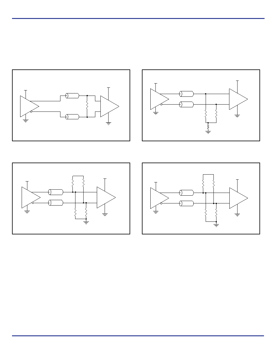
Differential Clock Input Interface
The CLK /nCLK accepts LVDS, LVPECL, SSTL, and other differential
signals. Both VSWING and VOH must meet the VPP and VCMR input
requirements. Figures 2A to 2D show interface examples for the
CLK/nCLK input driven by the most common driver types. The input
interfaces suggested here are examples only. Please consult with the
vendor of the driver component to confirm the driver termination
requirements. If the driver is from another vendor, use their
termination recommendation.
Figure 2A. CLK/nCLK Input
Driven by a 3.3V LVDS Driver
Figure 2C. CLK/nCLK Input
Driven by a 3.3V LVPECL Driver
Figure 2B. CLK/nCLK Input
Driven by a 3.3V LVPECL Driver
Figure 2D. CLK/nCLK Input
Driven by a 2.5V SSTL Driver
3.3V
R1
100
LVDS
CLK
nCLK
3.3V
Receiver
Zo = 50
Zo = 50
R3
125
R4
125
R1
84
R2
84
3.3V
Zo = 50
Zo = 50
CLK
nCLK
3.3V
LVPECL
Differential
Input
CLK
nCLK
Differential
Input
LVPECL
3.3V
Zo = 50
Zo = 50
3.3V
R1
50
R2
50
R2
50
CLK
nCLK
Differential
Input
SSTL
2.5V
Zo = 60
Zo = 60
2.5V
3.3V
R1
120
R2
120
R3
120
R4
120
发布紧急采购,3分钟左右您将得到回复。
相关PDF资料
ICS84314AY-02LFT
IC SYNTHESIZER 700MHZ 32-LQFP
ICS843156AKILF
IC CLK GENERATOR 32VFQFP
ICS843156AKLF
IC CLK GENERATOR 32VFQFP
ICS843202AYILF
IC SYNTHESIZER 680MHZ 32-LQFP
ICS843204AGILF
IC SYNTHESIZER LVPECL 48-TSSOP
ICS84320AY-01LN
IC SYNTHESIZER GP LVPECL 32-LQFP
ICS84320AYI-01LF
IC FREQ SYNTHESIZER 32TQFP
ICS843251AG-04LF
IC CLK GENERATOR LVPECL 8-TSSOP
相关代理商/技术参数
ICS8430S10BYI-02LFT
功能描述:IC CLK GENERATOR PLL 48TQFP RoHS:是 类别:集成电路 (IC) >> 时钟/计时 - 专用 系列:- 标准包装:1,500 系列:- 类型:时钟缓冲器/驱动器 PLL:是 主要目的:- 输入:- 输出:- 电路数:- 比率 - 输入:输出:- 差分 - 输入:输出:- 频率 - 最大:- 电源电压:3.3V 工作温度:0°C ~ 70°C 安装类型:表面贴装 封装/外壳:28-SSOP(0.209",5.30mm 宽) 供应商设备封装:28-SSOP 包装:带卷 (TR) 其它名称:93786AFT
ICS8430S10I-03
制造商:IDT 制造商全称:Integrated Device Technology 功能描述:Clock Generator for Cavium Processors
ICS8431-01
制造商:ICS 制造商全称:ICS 功能描述:200MHZ, LOW JITTER, LVPECL FREQUENCY SYNTHESIZER
ICS843101-312
制造商:ICS 制造商全称:ICS 功能描述:FEMTOCLOCKS⑩ CRYSTAL-TO-LVPECL 312.5MHZ FREQUENCY MARGINING SYNTHESIZER
ICS843101AG-312
制造商:ICS 制造商全称:ICS 功能描述:FEMTOCLOCKS⑩ CRYSTAL-TO-LVPECL 312.5MHZ FREQUENCY MARGINING SYNTHESIZER
ICS843101AG-312LF
制造商:ICS 制造商全称:ICS 功能描述:FEMTOCLOCKS⑩ CRYSTAL-TO-LVPECL 312.5MHZ FREQUENCY MARGINING SYNTHESIZER
ICS843101AG-312LFT
制造商:ICS 制造商全称:ICS 功能描述:FEMTOCLOCKS⑩ CRYSTAL-TO-LVPECL 312.5MHZ FREQUENCY MARGINING SYNTHESIZER
ICS843101AG-312T
制造商:ICS 制造商全称:ICS 功能描述:FEMTOCLOCKS⑩ CRYSTAL-TO-LVPECL 312.5MHZ FREQUENCY MARGINING SYNTHESIZER